FYI, Intel C2000 family of processors: System Fault may lead to dead system.

Ericloewe

Server Wrangler
Moderator
Joined
Feb 15, 2014
Messages
20,175
Hi...the LPC is a PCI-to-ISA connect regulator and is one of the two upheld BIOS boot areas; the C2000 can either boot from SPI (default) or LPC/ISA (set by means of outer sense pins at powerup). This is fixed in a venturing, and inquisitively the "fix" comprises of disposing of the capacity of muxing the LPC transport pins with GPIO - they as of now not become programming selectable. This is essentially ALL I've had the option to discover regarding the matter. There's a workaround which comprises of adding an outer 100 ohm resistor, yet it's not satisfactory what sticks this is added to. It's additional across two cushions on a connector on some Synology NAS units, so it's anything but a yield current limiter however in all likelihood a solid pullup or pulldown. This leads me to presume it truly goes on an arrangement sense pin. Intel hasn't made their "foundation level change" public. Following it out on a board is somewhat hard since the SoC is an enormous BGA bundle that would should be desoldered.

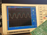
Does anybody find out about this? Like, for instance, where the resistor is added - specifically is it added to the LPC clock yields, or to the sense inputs?
Allow me to present a more readable version of what I think you're saying, for future readers who might struggle to understand, as I did, without full context:

C2000 can boot either from the LPC bus or from the SPI bus. This is selected [by applying a pull-up to the FLEX_CLK_SE0 / AH59 pin]. I suspect that the resistor fix is related to this.


My thoughts follow:

As it turns out, most systems do not boot from the LPC bus, but from SPI, which makes sense when you consider that SPI EEPROMs are everywhere, unlike LPC ROMs. In fact, the datasheet has this little gem:
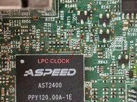
LPC Clock: These signals are the clocks driven by the processor to the LPC devices.
Each clock can support up to two loads.
Note: If the primary boot device is connected via the LPC interface,
it should use LPC_CLKOUT[0]. Using the LPC interface for the boot
device is not supported at this time and may not ever be supported by
this Intel product. Only use the SPI interface for boot device connection.

My first thought was "oh crap, they're using the LPC clock pin to choose whether to boot from SPI or LPC" - but that's wrong. There are two LPC clocks and neither of them is shared with this pin. They are LPC_CLKOUT0 / AG51 and LPC_CLKOUT1 / AM49.

So why the hell do systems cease to boot? My only hypothesis is that Intel is doing something weird with these clocks internally that breaks if the LPC Clock isn't being driven correctly.

I also considered that the systems might be booting, but failing early in the system firmware code because they can't reach LPC devices - namely the BMC (ASRock C2x50D4I boards also use a SuperIO, which I think Supermicro does without). I think we can discard this because I have a system that boots but cannot communicate with the BMC on the LPC once I apply the resistor fix on the LPC clock.

It's also vaguely possible that the BMC might somehow be holding the host CPU in reset in the absence of an LPC clock. It's difficult to tell without schematics (which the motherboard vendors keep under lock and key), datasheets (which ASpeed keeps under lock and key) or a straight answer about the workaround (which Intel keeps under lock and key).

Edit: Might everyone be using FLEX_CLK_SE0 for the LPC clock instead of the LPC_CLKOUT pins? I think that's what ASRock is doing, their manual mentions that the SuperIO is communicating at 33 MHz, which is only supported by the Flex Clocks, not the LPC.
That doesn't explain Supermicro, which does run the LPC bus at 25 MHz. But maybe Intel's reference design used that pin and everyone just ran with it, because why would they waste engineering hours for no gain?
 
Last edited:

Ericloewe

Server Wrangler
Moderator
Joined
Feb 15, 2014
Messages
20,175
Small update:

I tried to pull up the LPC data lines, but that did not improve the BMC comms.

In the meantime, I have an RMA approved by Supermicro and the seller is covering shipping to Supermicro in the Netherlands. I plan to ship off the motherboard on Wedensday, so in the meantime I might try to get a better look at the LPC signals and figure out if I can get the BMC to talk to the host.
 

Ericloewe

Server Wrangler
Moderator
Joined
Feb 15, 2014
Messages
20,175
Update time:

I sent off the board for RMA on schedule and ended up not having the time to do much more experimentation. It was delivered to Supermicro but I got no feedback until today - just before I was going to contact them for an update, I got an email from UPS that I have a delivery from them on the way. I guess that means that they repaired it or replaced it under the recall, since I wasn't asked to pay for anything.
More info on Tuesday when it arrives.
 

Ericloewe

Server Wrangler
Moderator
Joined
Feb 15, 2014
Messages
20,175
So, the A1SRi-2758F is back, nice and repaired. Seller included some dodgy RAM ("Mustang Memory", Hynix ICs, no readable SPD data) that won't boot without a careful application of voodoo dance.

Because reasons, I have also acquired a similar system with an A1SRi-2558F board and non-dodgy RAM. It still boots, but the host cannot reach the BMC. See attached scope shots, taken while the BMC flashing utility is trying to access the BMC - they're not single captures, the scope is actually rolling, but the signal just repeats what's shown here.

I'm not really sure what to make of this. I couldn't single-shot capture the traffic when the host tries to reach the BMC because keyboard activity (I tried different keyboards with no change) resulted in garbage (on all of the data lines) that prevented anything meaningful from being captured. I could see Lines 0 and 1 switching from input to output, but failing to be driven... But then why do they not start on the same clock cycle? Lines 2 and 3 seem to have some activity.

In the meantime, Wikipedia says something interesting about the LPC bus:
the bus is undriven and held high by the pull-up resistors
If true, this undermines the usual "it's the high-side of the totem-pole driver that's failing". Rather, it would be a weird failure mode in which the low-side driver (if there even is a high-side transistor!) is stuck partially on, sucking away the voltage from the weak pull-up, but off enough to allow a stronger pull-up to work. This could be modeled something like a parasitic resistance in parallel with the transistor, between source and drain, forming a voltage divider when the transistor is off (logic high output). On a nominal SoC, the parasitic resistance would be massive, resulting in the bus line being close to 3.3V. On a defective SoC, the parasitic resistance would need to be significantly smaller than the nominal pull-up (tens-hundreds of kOhm). If my measurements from post #158 are typical, with a ~200 Ohm strong pull-up bodge, this would imply a parasitic resistance in the 500 Ohm range. It also neatly explains why the SoC would be reading the Clock Output pin as low (i.e. LPC boot rather than SPI boot).

Figures:

Clock

Clock2.png


LPC bus (LAD0)

LAD0.png


LPC bus (LAD1)

LAD1.png


LPC bus (LAD2)

LAD2.png


LPC bus (LAD3)

LAD3.png
 

Ericloewe

Server Wrangler
Moderator
Joined
Feb 15, 2014
Messages
20,175
So, after going over the LPC specification, the SMBIOS Type 38 (IPMI) specification, the IPMI specification and the Parallel PCI specification, and after manually decoding what's on the bus (see previous post), and probing all easily-accessible LPC signals, I reached a conclusion:

All the LPC signals seem to be okay!

But then why do they not start on the same clock cycle?
Silly me from the past, you're triggering on the rising edge on a bus that rests at high!

When trying to reach the BMC, the SoC does an I/O read on the BMC's status port, whose address is defined in SMBIOS as 0x0ca2 + 1 (0x0ca3). On the LPC bus, this corresponds to the following (LFRAME is driven high unless otherwise indicated).
  1. 1 START clock cycle (LFRAME and LAD[3:0] driven low)
  2. 1 CT/DIR clock cycle (LAD[3:0] set to 0x0, representing the I/O Read Cycle Type)
  3. 4 Address clock cycles (LAD[3:0] set to 0x0, 0xc, 0xa, 0x3 - the BMC Status I/O Port)
  4. 2 TAR clock cycles (First LAD[3:0] is driven high, then supposedly tri-stated)
  5. 5 Sync clock cycles where crickets are heard on the bus
  6. Host gives up and does a reset of the BUS (LFRAME driven low for four cycles)
So, what does this mean? Well, either the BMC does not respond or it's unable to drive the bus. I won't say the latter option is impossible, but it doesn't seem very likely since there's nothing on the bus (not much of the Sync period is visible in the previous post, but it's all the same, it just stays at 3.3 V).

The BMC is still accessible over HTTP - I can't login because the default credentials won't work and neither do the credentials the seller dug up. Which leaves... somewhat-corrupted firmware? Physical damage to the BMC that doesn't affect the core or the Ethernet parts?

I guess the next step is to figure out where the BMC EEPROM is and to try to read it. Fun.
 

Ericloewe

Server Wrangler
Moderator
Joined
Feb 15, 2014
Messages
20,175
I came across a post I somehow missed with an awfully-compressed picture of Supermicro's fix on A1SRi boards. It's two new resistors that seem to be on completely different pins - so maybe they're pulling up two clock lines? And maybe the BMC actually uses the clock line that's not run to the TPM header.

Why use two clock lines? It's sort of expected that LPC devices will end up using the LPC clock for their own internal needs and operate synchronously. This wouldn't as much of an issue for the data lines because they would just terminate at the transceivers in the devices.
I guess that instead of specifying that devices cannot load down the clock too much, Intel just threw additional drivers onto their chipsets back in the day to compensate. Hell, maybe Intel even expected that this could turn into a problem and had OEMs spread out their LPC devices over the available clocks, even if it's just two devices (TPM and BMC).

Shamelessly copying the image to preserve it for posterity:

VbSeskik19c5zm2PxEYZz5E8.jpg


Yeah, that's not a fun soldering job!
 

RZSN

Cadet
Joined
Mar 3, 2023
Messages
5
That thread was very helpful in repairing my A1SAi-2750F that had the inoperable IPMI issue (and missed serial ports, etc) due to broken LPC channel to the BMC. It booted fine though. Especially the last post from @Ericloewe with the crude compressed image - is what was the fix I had applied now. The TPM clock was working okay (scope: cyan), while the BMC clock (scope: red - after repair) was initially at ground level. After adding two 150R pull-ups to nearby 3.3V rails as indicated in the crude picture, the thing fully works again. I had also finally identified the LPC clock testpoint near the Aspeed BMC chip. I knew it was ball B20, but could not trace it when it was deadly at ground. Hope this helps others, as it helped me! The BMC resistor is the harder part to solder, I did it without moving the original component, which would probably be safer - as there is a nearby testpoint.
 

Attachments

  • clock-signals.jpg
    clock-signals.jpg
    405.4 KB · Views: 218
  • a1sai-lpc-fix-pullups.jpg
    a1sai-lpc-fix-pullups.jpg
    615.1 KB · Views: 221
  • bmc-lpc-clock-testpoint.jpg
    bmc-lpc-clock-testpoint.jpg
    527.1 KB · Views: 226

Ericloewe

Server Wrangler
Moderator
Joined
Feb 15, 2014
Messages
20,175
Hell yeah, now we're talking, the pieces are all falling into place. Over the weekend, I'm going to take side-by-side pictures of my A1SRi-2758F and A1SRi-2558F and now I'm totally ordering a crapton of 0402s (because why not, they're cheap as... resistors?).
The TPM clock was working okay (scope: cyan)
Is the TPM clock waveform from before the repair or after? I find it interesting that it's not looking great, either while my unrepaired board has one clock line that looks basically unaffected (minus the dodginess from having wires running around to the probes at 25 MHz) and one clock line that is dead.
 
Last edited:

Ericloewe

Server Wrangler
Moderator
Joined
Feb 15, 2014
Messages
20,175
Also, how do I promote you out of the kiddy pool? There's no way in hell a first post of that caliber ends up being from a spammer.
 

RZSN

Cadet
Joined
Mar 3, 2023
Messages
5
Both measurements are after the repair, I have not saved the before ones, only saw that one of them is really missing. To me the working clock looked fine even on the TPM header - just with a significant over and undershoot.. on 10x probe. Not sure if my old scope is dying or I just did not find a proper ground on the board, so I skipped archiving that waveform. Do not judge the measurement as an absolute - its merely to show the difference between the two clocks - but yes, the TPM is unpopulated and the BMC makes a single load. Measurement point of red/cyan is at the newly installed pull-up resistors, which is same as the already present series resistors at source (CPU), but have not measured what they are.

Then I have also a C2550D4I (working) and C2750D4I (stuck at System initializing), on these I can cross-swap the BMC flash and/or BIOS and still the dead board is dead, and the working one is working. The LPC clock seems to run also to a SuperIO (nuvoton), and the failed one has a little smaller Vpp on it (using 100R-up/470R-down soldered at TPM header on both, lower than 100R makes that 2sec power cycle loop). Both bioses were re-configured (while inserted in the working board) to not wait for IPMI, so I do not really know what is the problem with that one. Shame that the better one of the two is the inoperable one.

Yeah, first poster, because (shhh.. I do not run TrueNAS), I am here for the hardware this time. I do hardware design and prototyping - FPGAs, image sensors, dreaming of own MOBOs and SSDs.. because oh boy, I have a huge collection of dead ones. If you need some more tests on any of the three boards I can do it as none are used yet.
 

Ericloewe

Server Wrangler
Moderator
Joined
Feb 15, 2014
Messages
20,175
The LPC clock seems to run also to a SuperIO (nuvoton)
Yeah, ASRock mysteriously figured they'd splurge for a SuperIO despite the BMC already having a SuperIO built in.
Yeah, first poster, because (shhh.. I do not run TrueNAS), I am here for the hardware this time.
Glad to have you anyway.
Then I have also a C2550D4I (working) and C2750D4I (stuck at System initializing), on these I can cross-swap the BMC flash and/or BIOS and still the dead board is dead, and the working one is working.
There are pictures out there of C2x50D4Is bodged repaired by ASRock with additional pull-ups on other signals, presumably the data lines. I can imagine the CPU waiting for the SuperIO to answer to something, but I haven't seen empirical evidence of the non-clock lines being affected by this bug.
 

RZSN

Cadet
Joined
Mar 3, 2023
Messages
5
There are pictures out there of C2x50D4Is bodged repaired by ASRock with additional pull-ups on other signals, presumably the data lines. I can imagine the CPU waiting for the SuperIO to answer to something, but I haven't seen empirical evidence of the non-clock lines being affected by this bug.
Can you point me to those images please ?

ad Waiting - besides the supermicro/asrock boards, I was experimenting with some HPE Moonshot CPU modules. There is an Avoton equipped model which I liked for the features it had (four so-dimms, 2.5 drive). The one I got had the AVR54 bug, and back then I had more time to play with it - so I hooked up a crude logic analyzer (from a Cypress FX3 devkit) to the SPI BIOS to see what it does. Decoding the SPI trace, it revealed the usual "extended boot" - reading soft-fuses, reading flash partition table, continuing with "classic x86 reset" vector of F000:FFF0 and about a dozen instructions later, it did a write to Port 80, that was routed through LPC (to an onboard MachXO2 fpga). After the "out,80" instruction there were no other fetches from the SPI flash.

So yes, the faulty LPC would block, yet I am not familiar with the "why" part. The Intel LPC specs looks like the host drives the bus and the device has to conform. But then there are some SYNC and wait states - so maybe the failure point is around that. I had no sense where the LPC signals are on the Moonshot board, so I could not logic-analyze the LPC itself (and it would be impossible with-out a working clock in first place).
 

Ericloewe

Server Wrangler
Moderator
Joined
Feb 15, 2014
Messages
20,175

RZSN

Cadet
Joined
Mar 3, 2023
Messages
5
Upper in that thread, you see a similar shape measurement as mine. I am a bit worried about using so strong loads (pull-ups), 120R is 27.5mA, with 50% duty cycle the load is 13.75mA-ish. But it can be regarded as necessary, to make the rising edge fast enough, for the given frequency and load. But considering the fix location on the Supermicro A1SAi, both lines had a series resistor close to the CPU, which may be a nice place to insert a true (push-pull) buffer, one with short propagation delay, and the short line from the CPU would be less capacitance, thus weaker pullup necessary (and the digital buffer will reshape the edge anyway). I think the clocks are in phase, so the working one can be used, and the other one can be just pulled up - if it happens to share a strap functionality. Will try this later maybe - but if people ran repaired boards for years, maybe I am just unnecesarily careful.
 

Ericloewe

Server Wrangler
Moderator
Joined
Feb 15, 2014
Messages
20,175
I agree with the concerns about the strength of the pull-up, it sounds like a lot of current for an I/O pin to be sinking. That said, I did some digging, and PCI clock buffers seem to be designed typically for a 50 mA absolute max sinking/sourcing capability. If that's representative of what Intel does inside the chipset/SoC, it should be bearable over time, if each pin can do the 50 mA independently.

I think the clocks are in phase, so the working one can be used, and the other one can be just pulled up - if it happens to share a strap functionality.
They have to be, since they're operating with the same bus lines.
 

Ericloewe

Server Wrangler
Moderator
Joined
Feb 15, 2014
Messages
20,175
A1SRi-2558F LPC Clock Comparison.png


Here's a comparison of the two clocks on my A1SRi-2558F, Yellow is the BMC clock at the test point, Magenta is the TPM header clock. Yellow is all over the place picking up all kind of crap, but the 25 MHz is there - keep on mind that Yellow is at 50 mV/div rather than 1 V/div.
 

Ericloewe

Server Wrangler
Moderator
Joined
Feb 15, 2014
Messages
20,175
As promised, here's a side-by-side comparison of a repaired and an unrepaired A1SRi.

Repaired, note the two bodged resistors (150 Ω) (between the right pad of R375 and right pad of the unpopulated R1731; between the bottom pad of R1578 and the top pad of the R1736) :

A1SRi-2758F Repaired.JPG


Unrepaired:

A1SRi-2558F Unrepaired.JPG


A1SRi-2758F Repaired annotated.jpg

EDIT:

Due to prior unfortunate events, I want to clarify that these images may be freely distributed with proper attribution (Please use the
URL for this post - https://www.truenas.com/community/threads/fyi-intel-c2000-family-of-processors-system-fault-may-lead-to-dead-system.50314/page-9#post-748036). Please refrain from posting potato-quality versions of these images. Thanks!
 
Last edited:

RZSN

Cadet
Joined
Mar 3, 2023
Messages
5

I did it same way as they - five resistors on TPM, to an uncovered trace (beeps to the 3.3V on TPM header) and two under the CPU from which one beeps to the IRQ tpm pin, and the other one I have not discovered, but might be the bmc clock. On the C2750D4I of mine.

What was another issue along the way, that I have experimented with other memories too much.. and it did not work until I did something.. well.. RTFM - and found there the memory population order. Which wants the first memory into the blue slot, on the board edge side... yet closer to the CPU. What an unnatural choice really! I always seen instructions to populate the farthest slot, as the little stub on the line is then from the unpopulated slot. I also mainly used the other memory channel solely - so my stick was in B2 - and moving it into A1 did the trick here. From that point I could check all my sticks, and eg A1+A2 (2DPC for A channel, with B unpopulated) did not work for me - the board turned itself off. Bringing in more sticks I am maxing out this second board with 4x4G that mix 1600 and 1333 within same channel (and it runs therefore at 1333).

So I can say, this thread and people did a wonderful job for me, two repairs in 2 days!
 

Ericloewe

Server Wrangler
Moderator
Joined
Feb 15, 2014
Messages
20,175
On one hand I get it, memory training is a pain and setting up the code to deal with any combination of DIMM slots takes time, money and ROM space, and all three are perpetually in short supply.
On the other hand, surely they could at least beep to let the user know the memory isn't working.
 

Ericloewe

Server Wrangler
Moderator
Joined
Feb 15, 2014
Messages
20,175
Oh my god, I am not doing this again without better magnification tools. My crappy El-Cheapo magnifier glass on a stand was not fun to use and I feel like I'm going to need glasses after this ordeal. I mean, the top resistor was fairly easy, although the result was very, very ugly. But the bottom one... holy crap.

Pictures tomorrow, because I'm way too tired to get the camera. Also, I need some mental distance between the time of such a disclosure to the public and the miserable work that was done.

But at least the BMC is talking over LPC again:

1678496820716.png


5 seconds after getting the HTML5 iKVM up, I realized I could've dealt with the upgrade from the ancient, HTML5-less firmware at a later time if I'd just SSH'd in to this live USB environment. Oh well.
 
Top